October 18, 200810 minutes
Tutorial Overview
In this example, we will develop a driver for the 16x2 character LCD on the ML505/6/7 board. The LCD driver will be mostly a Microblaze design, as opposed to being an IP design. The physical interface to the LCD will be made through a GPIO peripheral. The signal timing requirements of the LCD will be achieved by using a Timer peripheral. The functions contained in the software application will control what is shown on the LCD. The main function of the software application will provide a simple example of how to clear the display, write a message on the LCD and to change the cursor location.
The design is built on the interface specifications contained in the LCD datasheet. The connections to the FPGA are found on page 12 of the ML50x schematics. It is recommended that you read those documents before following this design.
This tutorial contains screenshots to guide you through the entire implementation process. Click on the images to view a higher resolution.
Requirements
Before following this tutorial, you will need to do the following:
Create the Basic Project
Follow these steps to create the basic project:
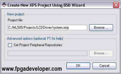
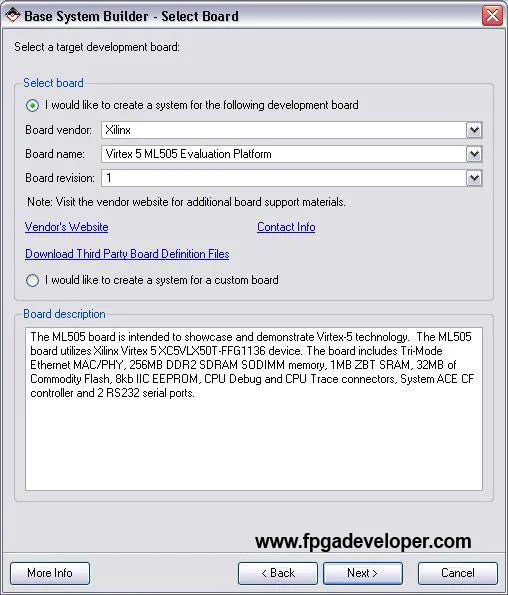
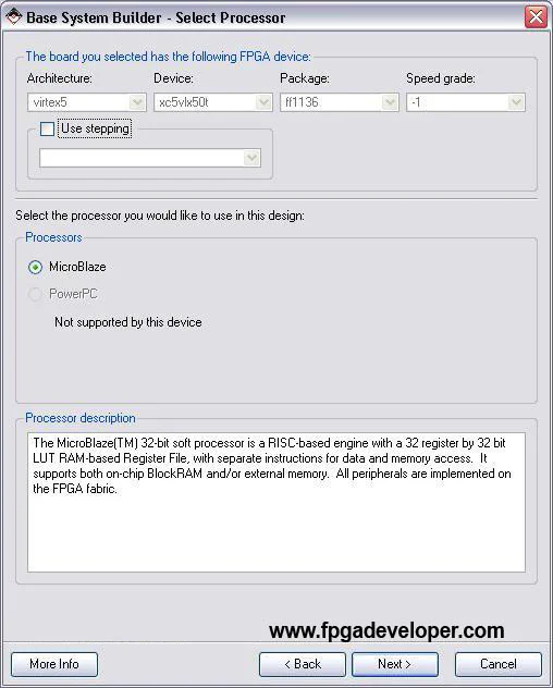
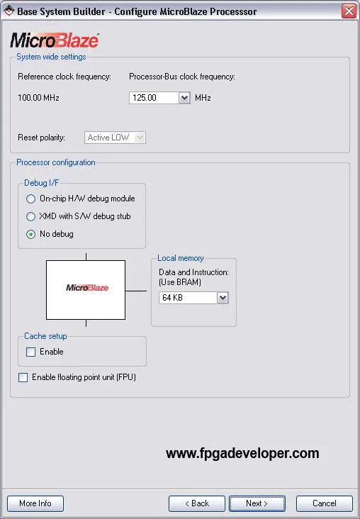
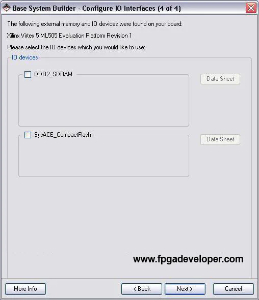
RS232_Uart_1 ticked and un-tick everything else.


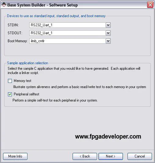
RS232_Uart_1 for both STDIN and STDOUT. Leave “Peripheral Test” ticked and un-tick “Memory Test”. Click “Next”.
Add the GPIO for the LCD
Now we will add a GPIO peripheral to allow the Microblaze to control the LCD.
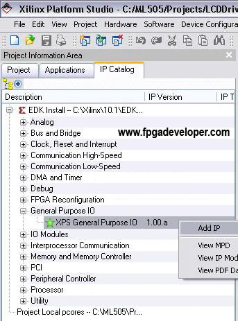
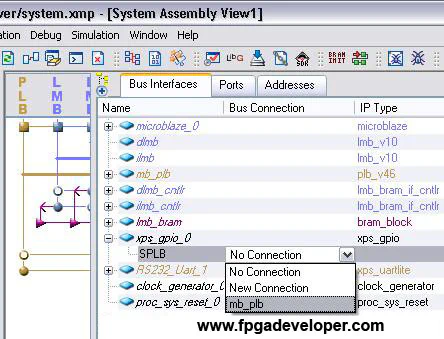
xps_gpio_0 tree and selecting mb_plb for the “SPLB” bus connection.
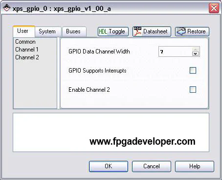
xps_gpio_0 instance. We can modify the instance parameters using this dialog box. type 7 for the “GPIO Data Channel Width” and click OK.
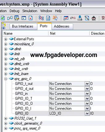
xps_gpio_0 tree.GPIO_IO net should display “No Connection”. Click on “No Connection” and type LCD_IO to give the net a name.
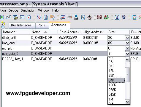
system.mhs file to include the new external port.xps_gpio_0 size drop-down menu and select 64K. Then click “Generate Addresses”. XPS automatically reconfigures the memory map and gives the GPIO peripheral a base address and a high address. It also automatically modifies the system.mhs file to update the IP address details.
We have now created an instance of the GPIO peripheral in our design. Later, we will modify the constraints file to connect the GPIO peripheral IO port to the LCD.
Add the Timer Peripheral
We now add a timer peripheral to the project to allow the Microblaze to measure time delays. A delay function will be used to create the required signal timing for the LCD interface. Follow these steps to add the peripheral:
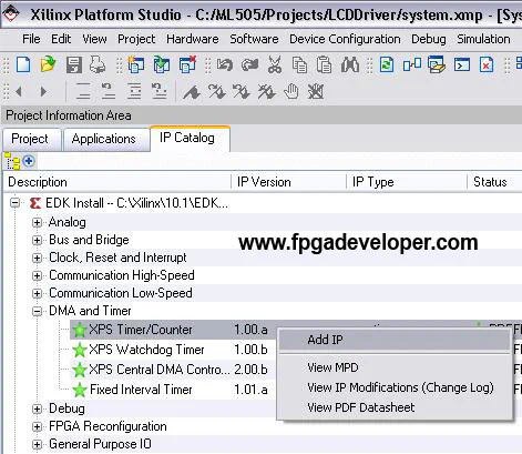
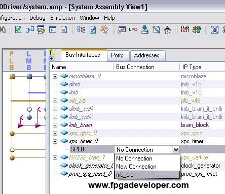
xps_timer_0 tree and selecting mb_plb for the “SPLB” bus connection.
xps_timer_0 size drop-down menu and select 64K. Then click “Generate Addresses”.
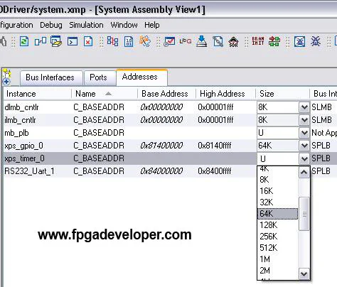
We have now created an instance of the Timer peripheral in our design.
Modify the Constraints (.UCF) File
The GPIO peripheral that we added to the design must be linked to the external pins on the FPGA that in turn connect to the LCD. The LCD interface consists of the 7 signals listed below. They are shown with pin description, pin name from the LCD datasheet, and the net name from the ML505 schematic. In brackets are the corresponding FPGA pins that they connect to on the ML505 board.
Follow these steps to add those pin locations to the constraints file:
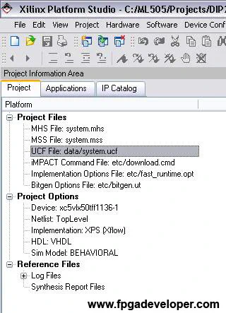
<
table width=“100%” border=“1”>
#### Module LCD_IO constraints

# LCD_FPGA_DB4
Net LCD_IO_pin<6> LOC = T9;
Net LCD_IO_pin<6> IOSTANDARD=LVCMOS33;
Net LCD_IO_pin<6> PULLDOWN;
Net LCD_IO_pin<6> SLEW=SLOW;
Net LCD_IO_pin<6> DRIVE=2;
# LCD_FPGA_DB5
Net LCD_IO_pin<5> LOC = G7;
Net LCD_IO_pin<5> IOSTANDARD=LVCMOS33;
Net LCD_IO_pin<5> PULLDOWN;
Net LCD_IO_pin<5> SLEW=SLOW;
Net LCD_IO_pin<5> DRIVE=2;
# LCD_FPGA_DB6
Net LCD_IO_pin<4> LOC = G6;
Net LCD_IO_pin<4> IOSTANDARD=LVCMOS33;
Net LCD_IO_pin<4> PULLDOWN;
Net LCD_IO_pin<4> SLEW=SLOW;
Net LCD_IO_pin<4> DRIVE=2;
# LCD_FPGA_DB7
Net LCD_IO_pin<3> LOC = T11;
Net LCD_IO_pin<3> IOSTANDARD=LVCMOS33;
Net LCD_IO_pin<3> PULLDOWN;
Net LCD_IO_pin<3> SLEW=SLOW;
Net LCD_IO_pin<3> DRIVE=2;
# LCD_FPGA_RW
Net LCD_IO_pin<2> LOC = AC10;
Net LCD_IO_pin<2> IOSTANDARD=LVCMOS33;
Net LCD_IO_pin<2> PULLDOWN;
Net LCD_IO_pin<2> SLEW=SLOW;
Net LCD_IO_pin<2> DRIVE=2;
# LCD_FPGA_RS
Net LCD_IO_pin<1> LOC = J17;
Net LCD_IO_pin<1> IOSTANDARD=LVCMOS33;
Net LCD_IO_pin<1> PULLDOWN;
Net LCD_IO_pin<1> SLEW=SLOW;
Net LCD_IO_pin<1> DRIVE=2;
# LCD_FPGA_E
Net LCD_IO_pin<0> LOC = AC9;
Net LCD_IO_pin<0> IOSTANDARD=LVCMOS33;
Net LCD_IO_pin<0> PULLDOWN;
Net LCD_IO_pin<0> SLEW=SLOW;
Net LCD_IO_pin<0> DRIVE=2;
Modify the Software Application
The software application controls the LCD interface signals by writing to the GPIO peripheral. It contains several functions for performing the signal sequences for writing characters to the LCD, moving the cursor, etc. To achieve the required signal timing, the application contains a delay function that uses the Timer peripheral.
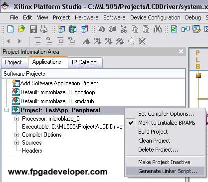
TestApp_Peripheral.c source file.<
table width=“100%” border=“1”>
#include "xparameters.h"
#include "xbasic_types.h"
#include "xgpio.h"
#include "xstatus.h"
#include "xtmrctr.h"

// Masks to the pins on the GPIO port

#define LCD_DB4    0x01
#define LCD_DB5    0x02
#define LCD_DB6    0x04
#define LCD_DB7    0x08
#define LCD_RW     0x10
#define LCD_RS     0x20
#define LCD_E      0x40
#define LCD_TEST   0x80

// Global variables

XGpio GpioOutput;
XTmrCtr DelayTimer;

// Function prototypes

void delay_us(Xuint32 time);
void delay_ms(Xuint32 time);
void gpio_write(Xuint32 c);
Xuint32 gpio_read(void);
void lcd_clk(void);
void lcd_set_test(void);
void lcd_reset_test(void);
void lcd_set_rs(void);
void lcd_reset_rs(void);
void lcd_set_rw(void);
void lcd_reset_rw(void);
void lcd_write(Xuint32 c);
void lcd_clear(void);
void lcd_puts(const char * s);
void lcd_putch(Xuint32 c);
void lcd_goto(Xuint32 line,Xuint32 pos);
void lcd_init(void);

// Main function

int main (void)
{
  Xuint32 status;

  // Clear the screen
  xil_printf("%c[2J",27);
  xil_printf("16x2 LCD Driver by Virtex-5 Resource\r\n");
  xil_printf("http://www.fpgadeveloper.com\r\n");

  // Initialize the Timer
  status = XTmrCtr_Initialize(&DelayTimer,
                                XPAR_XPS_TIMER_0_DEVICE_ID);
  if (status != XST_SUCCESS){
    xil_printf("Timer failed to initialize\r\n");
    return XST_FAILURE;
  }
  XTmrCtr_SetOptions(&DelayTimer, 1, XTC_DOWN_COUNT_OPTION);

  // Initialize the GPIO driver for the LCD
  status = XGpio_Initialize(&GpioOutput,
                                 XPAR_XPS_GPIO_0_DEVICE_ID);
  if (status != XST_SUCCESS){
    xil_printf("GPIO failed to initialize\r\n");
    return XST_FAILURE;
  }
  // Set the direction for all signals to be outputs
  XGpio_SetDataDirection(&GpioOutput, 1, 0x00);

  // Initialize the LCD
  lcd_init();

  // Example write to the LCD
  lcd_puts("http://www.fpga");
  lcd_goto(1,2);
  lcd_puts("developer.com");

  while(1){
  }
}

// Delay function (microseconds)
void delay_us(Xuint32 time)
{
  XTmrCtr_SetResetValue(&DelayTimer, 1, time * 125);
  XTmrCtr_Start(&DelayTimer, 1);
  while(!(XTmrCtr_IsExpired(&DelayTimer, 1))){}
  XTmrCtr_Stop(&DelayTimer, 1);
}

// Delay function (milliseconds)
void delay_ms(Xuint32 time)
{
  XTmrCtr_SetResetValue(&DelayTimer, 1, time * 125000);
  XTmrCtr_Start(&DelayTimer, 1);
  while(!(XTmrCtr_IsExpired(&DelayTimer, 1))){}
  XTmrCtr_Stop(&DelayTimer, 1);
}

// Write to GPIO outputs
void gpio_write(Xuint32 c)
{
  // Write to the GP IOs
  XGpio_DiscreteWrite(&GpioOutput, 1, c & 0x0FF);
}

// Read the GPIO outputs
Xuint32 gpio_read()
{
  // Read from the GP IOs
  return(XGpio_DiscreteRead(&GpioOutput, 1));
}

// Clock the LCD (toggles E)
void lcd_clk()
{
  Xuint32 c;
  // Get existing outputs
  c = gpio_read();
  delay_us(1);
  // Assert clock signal
  gpio_write(c | LCD_E);
  delay_us(1);
  // Deassert the clock signal
  gpio_write(c & (~LCD_E));
  delay_us(1);
}

// Assert the RS signal
void lcd_set_rs()
{
  Xuint32 c;
  // Get existing outputs
  c = gpio_read();
  // Assert RS
  gpio_write(c | LCD_RS);
  delay_us(1);
}

// Deassert the RS signal
void lcd_reset_rs()
{
  Xuint32 c;
  // Get existing outputs
  c = gpio_read();
  // Assert RS
  gpio_write(c & (~LCD_RS));
  delay_us(1);
}

// Assert the RW signal
void lcd_set_rw()
{
  Xuint32 c;
  // Get existing outputs
  c = gpio_read();
  // Assert RS
  gpio_write(c | LCD_RW);
  delay_us(1);
}

// Deassert the RW signal
void lcd_reset_rw()
{
  Xuint32 c;
  // Get existing outputs
  c = gpio_read();
  // Assert RS
  gpio_write(c & (~LCD_RW));
  delay_us(1);
}

// Write a byte to LCD (4 bit mode)
void lcd_write(Xuint32 c)
{
  Xuint32 temp;
  // Get existing outputs
  temp = gpio_read();
  temp = temp & 0xF0;
  // Set the high nibble
  temp = temp | ((c >> 4) & 0x0F);
  gpio_write(temp);
  // Clock
  lcd_clk();
  // Delay for "Write data into internal RAM 43us"
  delay_us(100);
  // Set the low nibble
  temp = temp & 0xF0;
  temp = temp | (c & 0x0F);
  gpio_write(temp);
  // Clock
  lcd_clk();
  // Delay for "Write data into internal RAM 43us"
  delay_us(100);
}

// Clear LCD
void lcd_clear(void)
{
  lcd_reset_rs();
  // Clear LCD
  lcd_write(0x01);
  // Delay for "Clear display 1.53ms"
  delay_ms(2);
}

// Write a string to the LCD
void lcd_puts(const char * s)
{
  lcd_set_rs();
  while(*s)
    lcd_write(*s++);
}

// Write character to the LCD
void lcd_putch(Xuint32 c)
{
  lcd_set_rs();
  lcd_write(c);
}

// Change cursor position
// (line = 0 or 1, pos = 0 to 15)
void lcd_goto(Xuint32 line, Xuint32 pos)
{
  lcd_reset_rs();
  pos = pos & 0x3F;
  if(line == 0)
    lcd_write(0x80 | pos);
  else
    lcd_write(0xC0 | pos);
}

// Initialize the LCD
void lcd_init(void)
{
  Xuint32 temp;

  // Write mode (always)
  lcd_reset_rw();
  // Write control bytes
  lcd_reset_rs();

  // Delay 15ms
  delay_ms(15);

  // Initialize
  temp = gpio_read();
  temp = temp | LCD_DB5;
  gpio_write(temp);
  lcd_clk();
  lcd_clk();
  lcd_clk();

  // Delay 15ms
  delay_ms(15);

  // Function Set: 4 bit mode, 1/16 duty, 5x8 font, 2 lines
  lcd_write(0x28);
  // Display ON/OFF Control: ON
  lcd_write(0x0C);
  // Entry Mode Set: Increment (cursor moves forward)
  lcd_write(0x06);

  // Clear the display
  lcd_clear();
}
Download and Test the Project
The software application simply initializes the LCD, clears the display and writes a message over the two lines. The LCD should look as shown in the image below.
You can download the project files for this tutorial and try it on your ML50x board. Please select the file corresponding to your board, right-click on it and select “Save Link As”. You can also download the project files here on GitHub.
Board
Virtex-5 Version
Project files
XC5VLX50T
XC5VSX50T
XC5VFX70T
XC5VLX110T