Useful Links
Update 2020-02-07: Missing Link Electronics has released their NVMe Streamer product for NVMe offload to the FPGA, maximum SSD performance, and they have an example design that works with FPGA Drive FMC!
Probably the most common question that I receive about our SSD-to-FPGA solution is: what are the maximum achievable read/write speeds? A complete answer to this question would require a whole other post, but instead for today I’m going to show you what speeds we can get with a simple but highly flexible setup that doesn’t use any paid IP.
[Read More]
IntelliProp Demos NVMe Host Accelerator on FPGA Drive
Early this year IntelliProp released a demo video of their NVMe Host Accelerator IP core running on the Intel Arria 10 GX FPGA Development board. As you can see in the video, they are using Opsero’s FPGA Drive product with the PCIe slot connector to interface the NVMe SSD to the FPGA board. They measured an impressive performance of around 2300MBps sequential write speed and 3200MBps sequential read speed.Demo of Intelliprop's NVMe Host Accelerator IP core
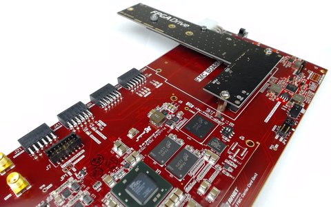
I’ve just done a video to demo Intelliprop’s NVMe Host Accelerator IP core on the Xilinx Kintex Ultrascale KCU105 dev board and the Samsung 950 Pro M.2 NVMe SSD. To connect them together I’ve used the FPGA Drive FMC plugged into the HPC connector to give us a 4-lane PCIe Gen3 interface with the SSD. The read/write speeds I got are simply incredible and line up very well with the numbers I wrote about in an earlier post.Connecting an M.2 SSD to FPGA Drive FMC
Just released a video showing how to connect an M.2 SSD to the FPGA Drive FMC.
NVMe Host IP tested on FPGA Drive
I’ve been totally overloaded with projects in the last couple months but I’m back with some really exciting news today. A few months back a company called IntelliProp, based in Colorado, released a NVMe Host Accelerator IP core for interfacing FPGAs with NVMe SSDs. This IP core allows reads and writes to be performed directly from the FPGA fabric, without the latency overhead of an operating system (read about the NVMe speed tests I did under PetaLinux).
[Read More]
FPGA Drive now available to purchase
Orders can now be placed for the FPGA Drive products on the Opsero website. Both the PCIe and FMC versions allow you to connect an M.2 PCIe solid-state drive to an FPGA development board and both can be purchased at the same price of $249 USD (solid-state drive not included).
The PCIe version has an 8-lane PCIe edge connector for interfacing with the PCIe blade (aka. goldfingers) of an FPGA development board.
[Read More]
Measuring the speed of an NVMe PCIe SSD in PetaLinux
With FPGA Drive we can connect an NVM Express SSD to an FPGA, but what kind of real-world read and write speeds can we achieve with an FPGA? The answer is: it depends. The R/W speed of an SSD depends as much on the SSD as it does on the system it’s connected to. If I connect my SSD to a 286, I can’t expect to get the same performance as when it’s connected to a Xeon.
[Read More]
At last! Affordable and fast, non-volatile storage for FPGAs
Let me introduce you to Opsero’s latest offering: FPGA Drive FMC, a new FPGA Mezzanine Card that allows you to connect an NVMe PCIe solid-state drive to your FPGA.
There’s got to be a better way. In the past, if you were developing an FPGA based product that needed a large amount of fast non-volatile storage, the best solution was to connect a SATA drive. Physical interfacing was pretty simple because all you needed was one gigabit transceiver.
[Read More]
FMC for Connecting an SSD to an FPGA
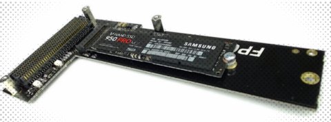
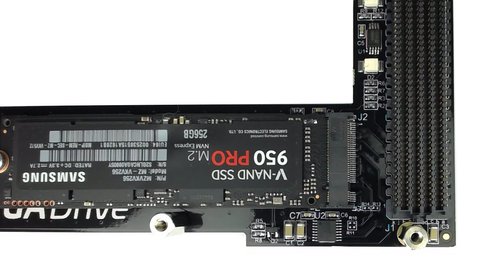
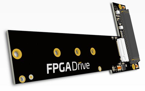
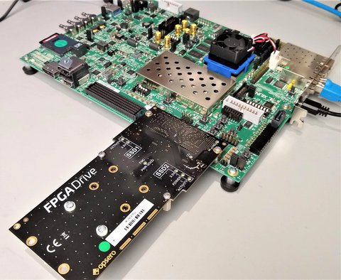
Here’s a first look at the FMC version of the FPGA Drive product, featured with the Samsung VNAND 950 Pro SSD. The FMC version can carry M-keyed M.2 modules for PCI Express and is designed to support up to 4-lanes. It has a HPC FMC connector which can be used on a LPC FMC carrier for a single-lane connection to the SSD, or a HPC FMC carrier to exploit the maximum throughput of a 4-lane connection.
[Read More]
Connecting an SSD to an FPGA running PetaLinux
This is the final part of a three part tutorial series on creating a PCI Express Root Complex design in Vivado and connecting a PCIe NVMe solid-state drive to an FPGA.
Part 1: Microblaze PCI Express Root Complex design in Vivado
Part 2: Zynq PCI Express Root Complex design in Vivado
Part 3: Connecting an SSD to an FPGA running PetaLinux (this tutorial)
In this final part of the tutorial series, we’ll start by testing our hardware with a stand-alone application that will verify the status of the PCIe link and perform enumeration of the PCIe end-points.
[Read More]