This video demonstrates how you would typically go about accelerating a Python function or algorithm on the Zynq-7000 with PYNQ. The function I chose to base this video on is the Finite Impulse Response (FIR) filter because the SciPy package contains the lfilter function which can be used for this purpose, and because the Xilinx IP catalog has a free FIR filter IP core. If you instead wanted to implement the accelerator in HLS, the process would be very similar, you would just have to design your accelerator with AXI-Streaming interfaces and ensure that the TLAST signals were properly managed.
[Read More]Create a custom PYNQ overlay for PYNQ-Z1
In this video tutorial we create a custom PYNQ overlay for the PYNQ-Z1 board. Probably the simplest PYNQ overlay possible, it contains one custom IP (an adder) with an AXI-Lite interface and three registers accessible over that interface: a, b and c. To use the IP we write a number to input registers a and b, and then we read the output register c which contains the sum of a and b. We create the IP in Vivado HLS, we then create the overlay in Vivado and bring the IP into our block design. Then we copy the overlay files (.bit and .tcl) over the network and onto the SD card of the PYNQ-Z1 board. Finally we open the Jupyter web application from a web browser and we write some Python code to test out our overlay and custom IP.
[Read More]Creating a custom AXI-Streaming IP in Vivado
The AXI-Streaming interface is important for designs that need to process a stream of data, such as samples coming from an ADC, or images coming from a camera. In this tutorial, we go through the steps to create a custom IP in Vivado with both a slave and master AXI-Streaming interface. The custom IP will be written in Verilog and it will simply buffer the incoming data at the slave interface and make it available at the master interface - in other words, it will be a FIFO. We’ll test the custom IP using a DMA which we’ll use to push streaming data into the IP and pull data out of the IP. We’ll use an SDK application to setup these DMA transfers and compare the sent data with the received data. The hardware we use for testing this will be the MicroZed 7010, so this is a Zynq-7000 design.
[Read More]Connecting an SSD to an FPGA running PetaLinux
This is the final part of a three part tutorial series on creating a PCI Express Root Complex design in Vivado and connecting a PCIe NVMe solid-state drive to an FPGA.
Part 1: Microblaze PCI Express Root Complex design in Vivado
Part 2: Zynq PCI Express Root Complex design in Vivado
Part 3: Connecting an SSD to an FPGA running PetaLinux (this tutorial)
In this final part of the tutorial series, we’ll start by testing our hardware with a stand-alone application that will verify the status of the PCIe link and perform enumeration of the PCIe end-points. We’ll then run PetaLinux on the FPGA and prepare our SSD for use under the operating system. PetaLinux will be built for our custom hardware using the PetaLinux SDK and the Vivado generated hardware description. Using Linux commands, we will then create a partition, a file system and a file on the solid-state drive.
[Read More]Zynq PCI Express Root Complex design in Vivado
This is the second part of a three part tutorial series in which we will create a PCI Express Root Complex design in Vivado with the goal of connecting a PCIe NVMe solid-state drive to our FPGA.
Part 1: Microblaze PCI Express Root Complex design in Vivado
Part 2: Zynq PCI Express Root Complex design in Vivado (this tutorial)
In this second part of the tutorial series, we will build a Zynq based design targeting the PicoZed 7Z030 and PicoZed FMC Carrier Card V2. In part 3, we will then test the design on the target hardware by running a stand-alone application which will validate the state of the PCIe link and perform enumeration of the PCIe end-points. We will then run PetaLinux on the FPGA and prepare our SSD for use under the operating system.
[Read More]Microblaze PCI Express Root Complex design in Vivado
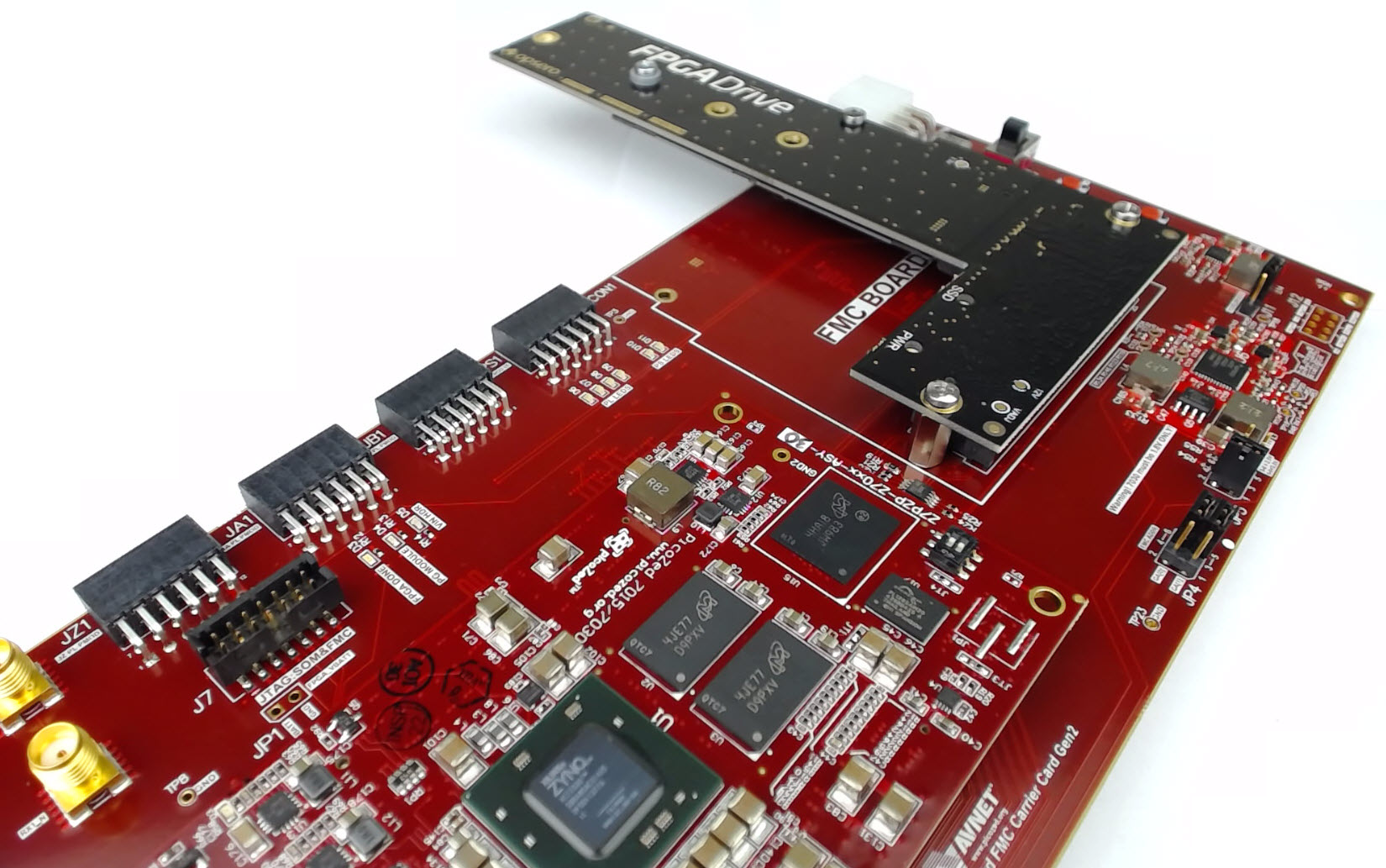
This is the first part of a three part tutorial series in which we will go through the steps to create a PCI Express Root Complex design in Vivado, with the goal of being able to connect a PCIe end-point to our FPGA. We will test the design on hardware by connecting a PCIe NVMe solid-state drive to our FPGA using the FPGA Drive adapter.
Part 1: Microblaze PCI Express Root Complex design in Vivado (this tutorial)
[Read More]Running a lwIP Echo Server on a Multi-port Ethernet design
Tutorial Overview
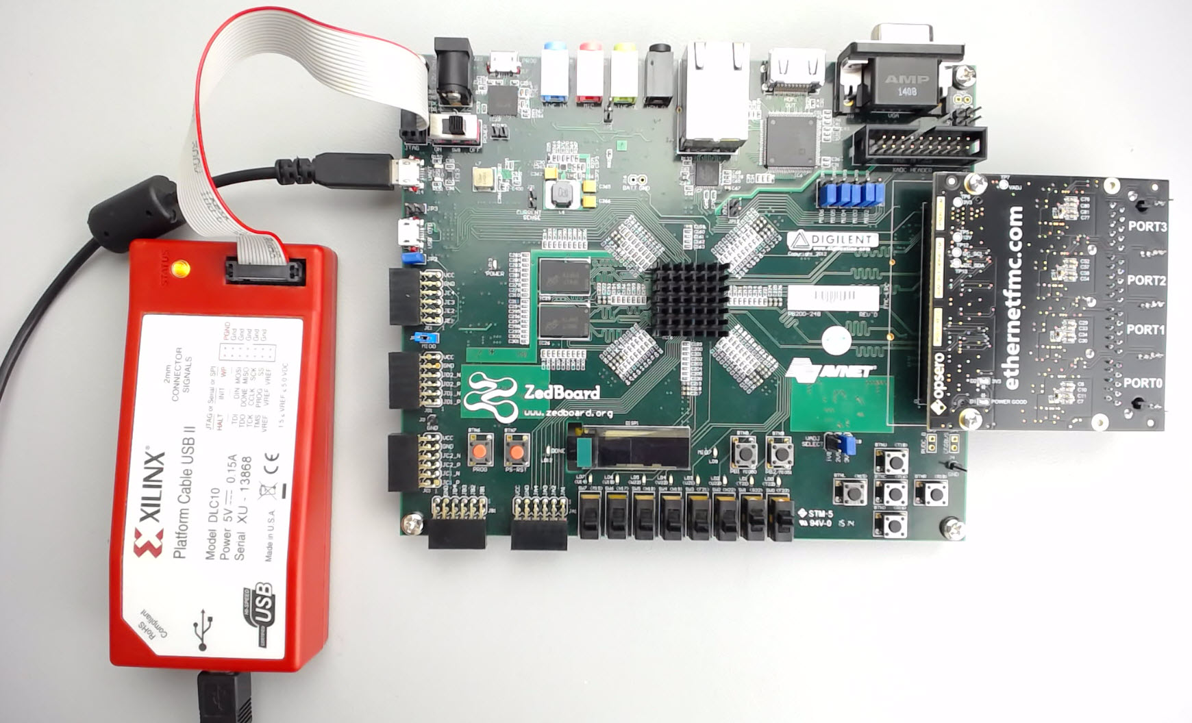
This tutorial is the follow-up to Using AXI Ethernet Subsystem and GMII-to-RGMII in a Multi-port Ethernet design. In this part of the tutorial we will generate the bitstream, export the hardware description to the SDK and then test the echo server application on our hardware. The echo server application runs on lwIP (light-weight IP), the open source TCP/IP stack for embedded systems. Our hardware platform is the Avnet ZedBoard combined with the Ethernet FMC.
[Read More]Using AXI Ethernet Subsystem and GMII-to-RGMII in a Multi-port Ethernet design
Tutorial Overview
In this two-part tutorial, we’re going to create a multi-port Ethernet design in Vivado 2015.4 using both the GMII-to-RGMII and AXI Ethernet Subsystem IP cores. We’ll then test the design on hardware by running an echo server on lwIP. Our target hardware will be the ZedBoard armed with an Ethernet FMC, which adds 4 additional Gigabit Ethernet ports to our platform. Ports 0 to 2 of the Ethernet FMC will connect to separate AXI Ethernet Subsystem IPs which will be configured in DMA mode. Port 3 of the Ethernet FMC will connect to GEM1 of the Zynq PS through the GMII-to-RGMII IP, while the on-board Ethernet port of the ZedBoard will connect to GEM0.
[Read More]Using the AXI DMA in Vivado

Update 2017-10-10: I’ve turned this tutorial into a video here for Vivado 2017.2. In a previous tutorial I went through how to use the AXI DMA Engine in EDK, now I’ll show you how to use the AXI DMA in Vivado. We’ll create the hardware design in Vivado, then write a software application in the Xilinx SDK and test it on the MicroZed board (source code is shared on Github for the MicroZed and the ZedBoard, see links at the bottom).
[Read More]Creating a custom IP block in Vivado
Update 2017-11-01: Here’s a newer tutorial on creating a custom IP with AXI-Streaming interfaces
Tutorial Overview
In this tutorial we’ll create a custom AXI IP block in Vivado and modify its functionality by integrating custom VHDL code. We’ll be using the Zynq SoC and the MicroZed as a hardware platform. For simplicity, our custom IP will be a multiplier which our processor will be able to access through register reads and writes over an AXI bus.
[Read More]