U.2 NVMe SSDs are the types of drives that are commonly used in enterprise servers and data centers. Compared to M.2 NVMe SSDs, which are more commonly found in consumer devices, U.2 drives are physically bigger, using the same form factor as the 2.5 inch SATA SSDs. The bigger form factor allows U.2 drives to consume more power and thus deliver higher sustained performance than their equivalent M.2 versions. This performance advantage is the reason why U.2 SSDs are becoming more popular in FPGA applications.
In this post I’m going to introduce our new product, the MCIO PCIe Host FMC. It’s a solution for connecting U.2 NVMe SSDs to FPGA and adaptive SoC development boards. That’s it’s primary use-case but we designed it to have the potential to be used in a multitude of other applications requiring cabled PCIe interconnects.
M.2 vs U.2
M.2 and U.2 NVMe drives both provide non-volatile data storage, and both interface with the host through a 4-lane PCIe bus. The major difference is their physical size.
| M.2 NVMe SSD | U.2 NVMe SSD | |
|---|---|---|
| Form factor | Small and slim circuit board | 2.5-inch drive |
| Interface | 4-lane PCIe | 4-lane PCIe |
| Typical use | Laptops, desktops, small-form-factor systems | Enterprise servers, data centers, workstations |
| Advantages | Small, lower power | Better thermal management, better performance |
The larger physical size of the U.2 drives allows them to better dissipate heat, which enables them to use more power to achieve higher performance. Looking at it the other way, the M.2 drives' smaller physical size limits their ability to dissipate heat, requiring them to throttle performance to consume less power and avoid overheating.
So how much “higher performance” can we expect from U.2 SSDs? How much does all of this M.2 thermal throttling add up to in terms of lost performance? These are not simple questions to answer because they depend on the drives being used, the conditions they are operating under and the system that is working them. The bad news: I don’t yet have an answer. The good news: Missing Link Electronics is currently working on an answer, for a specific setup, using the MCIO PCIe Host FMC and their proprietary NVMe Streamer IP. I’ll post those results when they become available.
Let’s talk now about MCIO.
Mini Cool Edge IO
Mini Cool Edge IO (MCIO) is a compact, high-speed I/O connector system developed by Amphenol. It’s designed with a slim form factor for use in space-constrained networking and server applications. MCIO supports high-speed signaling of up to 64G PAM4 and PCIe Gen6 (64Gbps per lane) over cables of up to 1m (3.3 ft) in length. Note that FMC/FMC+ connectors are only rated to 28Gbps, so they can’t exploit all of that bandwidth, but I’m sure that Samtec will catch up to it soon enough.
The photo below shows the MCIO PCIe Host FMC connected to an 8i MCIO to 2x U.2 adapter. The adapter that I’ve shown is from C-Payne and costs 75 Euros or about $80 USD. Two U.2 NVMe SSDs can be connected to an FMC carrier using this setup. Notice that the SSD power is supplied through a 4-pin Molex connector that is built into the cable.

We could have designed a U.2 to FMC adapter, but MCIO is a much better solution and here is why:
- Cables are better. There is an abundance of relatively cost effective MCIO-to-U.2 cables on the market (like this one from C-Payne). A cabled solution
is better for this because:
- U.2 drives are big with respect to the size of an FMC card. A U.2-to-FMC adapter would have been mechanically awkward. Using an MCIO cable gives us the flexibility to position the SSD wherever it makes the most sense, enabling better thermal management and a more mechanically robust overall system design.
- U.2 drives typically require more power than the FMC standard is designed for. MCIO cables offer a convenient way for us to provide power to the drive from an external supply that is independent of the FPGA board.
- Alternate applications. MCIO opens the door to using this product in many other applications and that’s what I think is most
exciting about this product. Here are some of the obvious alternate applications:
- Cabled FMC to PCIe interconnects as shown in the photo below. The MCIO PCIe Host FMC could be used to connect an FPGA board to a PCIe card via cable. This requires an MCIO-to-PCIe Receptacle adapter like the one shown in the photo and a straight-through 8i MCIO cable.
- A lot of server motherboards these days are built with MCIO connectors, and many of them can be used to connect with hardware accelerators - including FPGA-based ones. With our soon-to-be-released sister product, the MCIO PCIe Device FMC, you will be able to connect FPGA and adaptive SoC dev boards to these servers through a high-bandwidth and convenient cabled interface.
- Another potential application for this FMC card would be to connect two FPGA boards through their FMC connectors. Again, for this one, we would need the MCIO PCIe Device FMC.

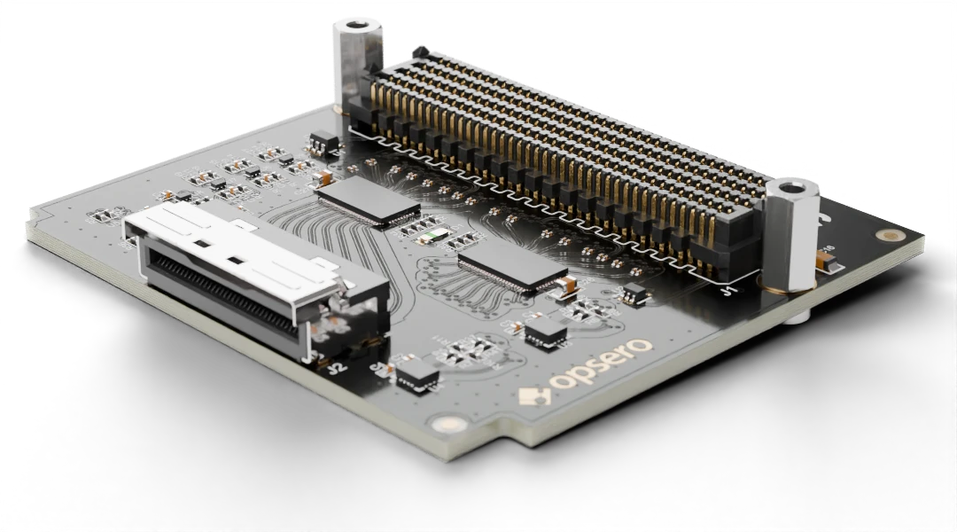
The MCIO PCIe Host FMC has a 74-pin MCIO connector with 8 gigabit transceiver lanes + side-band signals. The pin assignment follows the SFF-9402 standard and it is configured to be the host (aka. root port). The side-band signals include 100MHz reference clocks, PCIe reset signals, I2C buses and device present signals. When using an MCIO-to-U.2 adapter such as the one shown earlier, each U.2 SSD connects to 4 gigabit transceiver lanes and a set of each of the sideband signals.
Redrivers
The MCIO PCIe Host FMC has 2x TI DS320PR810 redrivers, one for the transmit path and another for the receive path. Redrivers are like amplifiers that boost the strength of the higher frequencies in the signal, compensating for the attenuation that those frequencies typically incur when traveling across a lossy channel like a cable or PCB traces. Redrivers allow the signal to travel longer distances and/or over more lossy channels, than would have been possible without equalization.
The TI DS320PR810 redrivers have registers, accessible over I2C, that allow configuration of the equalization settings. This means that we can change the equalization settings to suit our setup, the cable(s) that we are using, the traces on the FPGA board and the device we are connecting to. The default settings work fine for a 50cm cable and link speeds of up to PCIe Gen4.
Redrivers make this a much more versatile and useful product. We expect that people will want to use different kinds of cables and adapters with this product, as those options become available.
Board design
For those of you who are interested in the board design, I share some details and images below. But first…
If you let me go off track here for a second, I have to give a mention to Blender. This tool is my discovery of the year and it blows my mind that it is free software (although I have donated). I’ve always found electronic designs to be like artworks. It’s one of the reasons why I love my job - I feel like I get to make art all the time, albeit practical and functional art. The problem is that most if not all PCB CAD software offers us no way to present our work in a visually appealing way. Altium is not the exception. The following images were rendered in Blender and I look forward to using it more to create better visuals in my blog posts, documentation and websites.
…Back to the board. In the image below we can see the two redrivers, one for transmit and one for receive. Eight differential traces run into and out of each of them. You can also see the AC coupling capacitors that sit on those traces - in the tiny 0201 package so that their pads and separation make minimal impact to the trace dimensions. Redrivers will compensate for the insertion loss of a long trace, but they wont help with discontinuities, so we need to make sure that the impedance is maintained along the whole path as much as possible. The redrivers won’t help if we screw up the P/N length matching either.

Now in the image below we can see the TX gigabit traces leading to the MCIO connector. The RX gigabit traces, seen in the top left part of the image, need to change layer to get there, so they use an inner signal layer. In the lower part of the image, we can see 3x I2C bus voltage translators, one logic inverter, one 100MHz clock oscillator, the EEPROM and one I/O expander that we use in the production test. We designed this board with voltage translators so that it would support the I/O voltages of all FPGA and adaptive SoC devices on the market (specifically 1.2 - 3.3VDC).

In this next image, we get a better look at the high-speed differential traces going into and out of the redrivers. Notice that the traces are curved, they don’t use sharp angles. When these traces transition to another layer, the signal vias are surrounded by four ground return vias. Although it’s not visible in the image, the signal vias have a race-track style antipad that voids each of the copper layers through which the vias pass. These vias are also backdrilled from the bottom side of the board, to remove the stubs.

To make this last image, I made everything invisible except for the copper layers. It’s not visually accurate because I used an ENIG color/texture on ALL of the copper, not just on the exposed parts of the outer layers. In reality most of the copper would be more of a brownish color with a matte finish and probably wouldn’t look as nice. Anyway, I think this image looks interesting but it also reveals one of the limitations of Altium’s export feature: It hasn’t properly exported the detail in the first ground plane, the one just below the top layer (nor any of the internal plane layers for that matter). How do I know? For one, the via antipads should be race-track shaped. For two, there should be ground voids underneath the coupling capacitors. I wonder if KiCad’s export feature can do better.

Coming next
In the coming weeks I’m going to work this product into our popular Github repo (240 stars and counting!) so that you can get it working with one of several FPGA and adaptive SoC development boards. The product is available to buy from the Opsero website although not yet from Digi-Key (to be updated soon!).
