Title here
Summary here
High-speed Ethernet connectivity for FPGAs
July 16, 202410 minutes

In the next few days I will kick off the launch of another new Opsero FMC product: the Quad SFP28 FMC. This FMC card has 4x SFP28 slots that are compatible with SFP, SFP+ and SFP28 modules. The FMC and the reference designs that we are currently developing will enable 4x 10G/25G Ethernet links on a multitude of FPGA/MPSoC/RFSoC development boards including the newer Versal ACAP boards. We’ve already pushed working 10G/25G designs to the Github repo for the ZCU104, ZCU102, ZCU106, ZCU111 and ZCU208 with more coming soon.
Update 2024-10-07: The Github repo now has working reference designs for the Versal boards VCK190, VMK180, VEK280 and VPK120.
At the top of this post we see the top side of the board, where all of the components are mounted. Most of those ICs are the level translators, but we can also see the I2C switch and the jitter-attenuating clock multiplier. If you want to see which parts are which, just checkout this part of the datasheet.
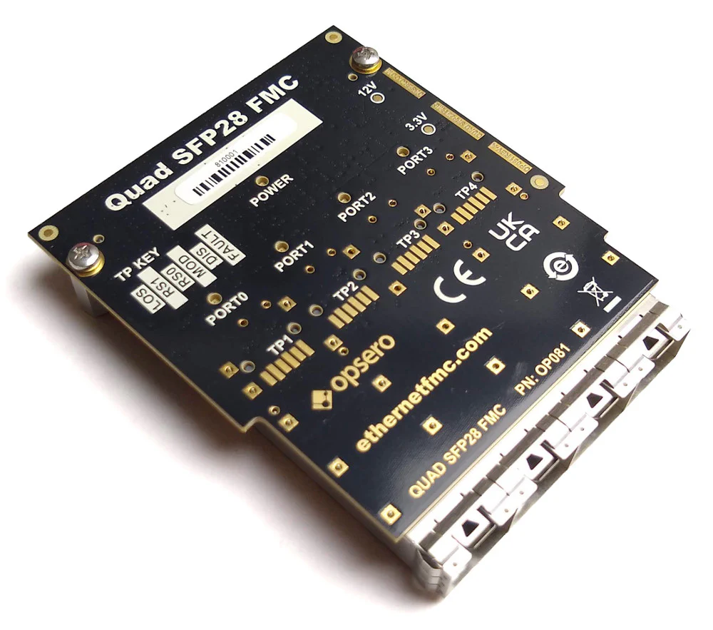
The image below shows the bottom side of the board where we’ve placed most of the labelling, the test points and the LEDs. Note that the LEDs are actually bottom entry and they are placed on the top-side of the board - we do this to eliminate one step of the assembly process, and also to make the board a bit more robust.
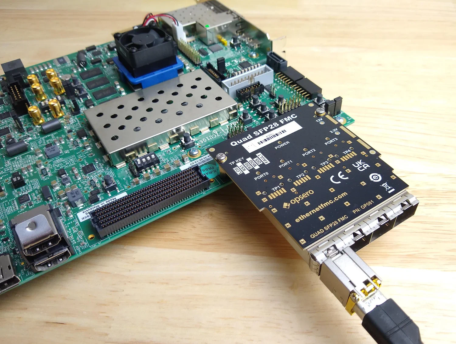
The image below shows how it looks when attached to the Versal AI Edge VEK280 development board with two optical SFP28 modules for 25G Ethernet. On this platform, we can achieve 4x 25G Ethernet links.
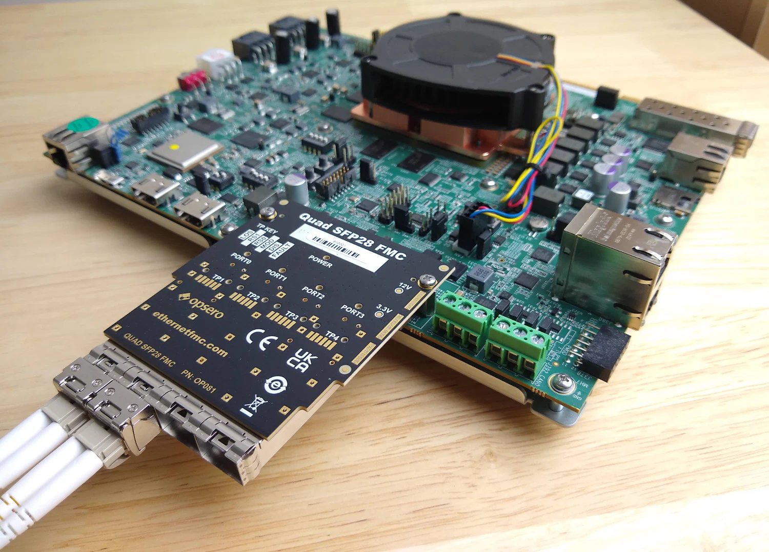
In the next image we see the FMC mated with the Zynq UltraScale+ ZCU106 development board with a single SFP28 module for 10G Ethernet over copper (RJ45). The gigabit transceivers on this platform can only support up to 10G Ethernet, but you could run other protocols up to 16Gbps over a DAC or optical fiber.
There are already a few SFP FMC cards on the market, so we decided to bring some new things to the table:
SFP28 (Small Form-Factor Pluggable 28), is a high-speed optical transceiver specification that is used in data communication and networking applications. You’re probably already familiar with the SFP and SFP+ transceiver modules, these are compact, hot-swappable devices, about the size of a finger. They are very commonly used in network infrastructure because they support high bandwidth and low latency while also supporting different physical links such as optical fiber and copper. SFP28 is an enhanced version of SFP+, designed for higher data rates (up to 28 Gbps, hence the “28” in SFP28). SFP28 transceiver modules are suitable for 25 Gigabit Ethernet (25GbE) applications.
The best thing about SFP28 is that the socket is backwards compatible with SFP and SFP+ modules. That’s why we used SFP28 on this FMC.
This is the first Opsero product to be designed for 28Gbps serial links. On our path to achieving this, we benefited greatly from the lessons learned (and shared) by Telian, Rowett and Teplitsky in their DesignCon2023 paper on PCIe Gen5 Signal Integrity. Here are some of the details for those who are working on similar designs:

To give you an idea of the cost of these design choices, for us, the board material choice combined with the backdrilling requirement increased the cost of the bare PCB by about 4x compared to using FR4 (180Tg) without backdrilling. This of course depends on the quantities that you purchase but I think that gives you a fair idea if you’re considering making these choices for your own designs.
Another factor to consider if you’re designing a board like this is that FPGA gigabit transceivers typically have a digital front end (DFE). In my experience the DFE in Xilinx AMD devices can effectively compensate for some amounts of insertion loss and certain discontinuities. It can make sense in some cases to go with lower cost materials and lean on the DFE - but of course whether this is feasible for you depends on many factors and needs to be determined on a case-by-case basis.
Finally on this point, you should note that not all of the Xilinx AMD devices have transceivers that can operate at 28Gbps. Here is a list of some of the dev boards that can do 28Gbps and have an FMC/FMC+ connector to support the Quad SFP28 FMC:
They’re all expensive of course!
Synchronous Ethernet (SyncE) is used when the nodes of a network require precise synchronization. Without going overboard, I’ll just explain what it is in basic terms so that I can then explain the purpose of the jitter-attenuating clock multiplier and how it’s normally used in an FPGA based SyncE system.
In a SyncE network, you basically have a master node that distributes the system clock through the network so that every node is operating with a clock that is synchronous to every other node. In order to achieve this, the nodes need to be able to recover the clock from the incoming (RX) serial link, clean the jitter and then use that clean recovered clock as it’s own transmit clock. Downstream nodes do the same thing until all nodes in the network are synchronous.
It sounds simple but in fact there is a technical challenge here that requires some specialized clocking hardware. The problem is that the network nodes cannot hold off all transmission until the system clock “flows” down the network to them - synchronous or not, they need to have a transmit clock at all times. Also there is the possibility of nodes going down or being disconnected in which case you don’t want the healthy nodes to suddenly stop transmitting too. The solution to this is that each node needs to have a clocking system that can do three things: (1) generate it’s own independent transmit clock, (2) recover and clean the receive clock, and (3) be able to switch between these two clocks at the right time and in a clean way that wont lock up the transmitter.
That is, in my own simple terms, the purpose of the jitter-attenuating clock multiplier ( Si5328) that we have added to the Quad SFP28 FMC. To use it in an FPGA system, we first set it up to drive the gigabit transceivers with a free-running clock (our transmit signal is synchronous to this clock). Then we take the recovered clock from the gigabit transceiver (which is synchronous to the receive signal), and use clock forwarding to send this clock to the Si5328 through specific pins on the FMC connector. The Si5328 on the Quad SFP28 FMC performs jitter-attenuation on this recovered clock. When it is determined that the recovered clock is stable, the Si5328 output can be switched over from the free-running clock, to the jitter-attenuated recovered clock. Once that switch has been made, our transmit clock is synchronous to the receive clock and we are propagating the clock through the network.
Newer devices like the Versal ACAP are not able to support the higher FPGA I/O voltages that the older devices once did. To give you an example, the maximum VADJ voltage supported by the VCK190 is only 1.5V. On the other hand, the minimum VADJ supported by the KC705 is 1.8V. This means that if you’re designing an FMC card and you want it to work on a wide range of development boards, it needs to work with a range of I/O voltages. For this reason we designed the Quad SFP28 FMC with voltage translators and we’re going to design all of our FMCs this way in the future.
What signals need translating? On this product, the I2C bus and SFP I/O connect to FPGA I/O pins and thus need translation. The gigabit transceivers don’t need it, they are independent of the I/O banks and VADJ. For an FMC card in general, what needs translation is all of the FPGA I/O pins: LA00-LA33, HA00-HA23 and HB00-HB21. A customer once asked me why we didn’t have a stackable “translator FMC” product that would allow any FMC to be used at any VADJ voltage. It would definitely be nice to have, but the problem is that translators are specific to the type of I/O being used. A translator for open-drain signals like I2C works completely differently to a translator that is designed for RGMII signals, or LVCMOS. As every FMC card uses the I/O pins for different signal standards in different combinations, it’s impossible to design a single translator FMC to suit them all.
As I mentioned earlier, we’re currently working on the 10G/25G Ethernet ref design but we have plans to do much more.
If you do any PCB layout for high-speed signals (10GHz+), the following papers might be of interest to you.