Ten years ago, almost to the day, I launched the Opsero Ethernet FMC. To my delight and surprise, many of our customers are still buying them today. Gigabit Ethernet still finds many uses in FPGA designs today, because it is simple to setup, the cabling is easy to buy and install, the throughput is ample for many applications and it is extremely versatile.
This year, I felt that it was time to upgrade our Ethernet FMC offering, so we’ve launched two new products: Quad SFP28 FMC which I have introduced to you in earlier posts (here and here), and Ethernet FMC Max, which I would like to introduce to you in this post.
Take a look
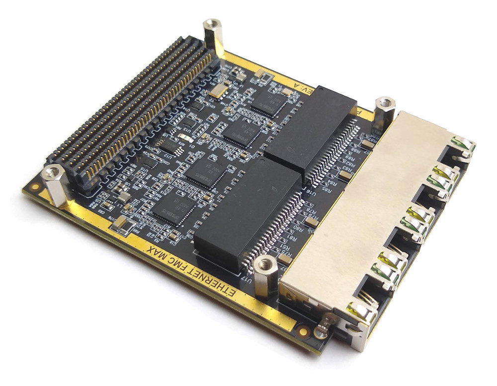
In the photo below we see the top side of the board where most of the components are mounted. On the very left is the quad RJ45 connector which sits comfortably under the 10mm clearance between the carrier board and FMC card. Moving to the right, those two black rectangular blocks are Ethernet magnetics modules. Then in the middle of the board we can see the four black QFNs: Texas Instruments DP83867CS Ethernet PHYs. Between the PHYs and the FMC connector on the right, we can see the clock oscillator, the EEPROM, level translators and two buck converters. If you want a more detailed look at the parts, just checkout this part of the datasheet.

The image below shows the bottom side of the board where we’ve placed most of the labelling and the test points. Note that the single power LED is visible from the bottom side. We use bottom entry LEDs on most of our FMC products to keep them on the side of the board that is more protected (the top side), while lighting-up on the side that faces upwards in normal use (the bottom side!).

In the next image we see the FMC mated with the Versal AI Edge VEK280 development board with two CAT5 cables plugged into it. When designing this product and the Quad SFP28 FMC, we paid special attention to making sure that they would be fully compatible with Versal ACAP. The AMD Xilinx Versal evaluation boards can only support a VADJ voltage between 1.2V and 1.5V, which is lower than a lot of existing FMC cards have been designed for.

SGMII Benefits
The table below shows a basic comparison between the original Ethernet FMC and the new Ethernet FMC Max in terms of the MAC interface and the FMC connector used.
| Product | MAC Interface | Gigabit transceivers required | Pins per interface | FMC |
|---|---|---|---|---|
| Ethernet FMC (original) | RGMII (parallel) | NO | 14-pins | LPC |
| Ethernet FMC Max | SGMII (serial) | YES | 4-pins | HPC |
The original Ethernet FMC uses 4x RGMII interfaces and we made that design choice so that it could support low pin-count (LPC) FMC carriers such as the Avnet ZedBoard. These days, most of the new FPGA/MPSoC boards being released have gigabit transceivers and high-pin-count (HPC) FMC connectors or even the bigger FMC+ connectors. We designed the Ethernet FMC Max with SGMII interfaces because they are a much better alternative to RGMII when you have the option to use gigabit transceivers. In FPGA designs, these are some of the advantages of SGMII over RGMII:
- Easier timing closure: RGMII interfaces are more complicated to implement on FPGA I/O pins. Different devices require different implementations, some devices require specific pins to be used. In general, pin selection and timing closure for RGMII interfaces is more of a challenge than SGMII.
- Better PCB layout: RGMII interfaces require a lot more traces than SGMII interfaces, and they must be length matched. The differential serial traces of an SGMII interface are easier to route, require less room and have further reach than RGMII.
- Superior EMC: Serial differential signalling in SGMII has inherently higher immunity to external noise and generates less electromagnetic interference than RGMII.
Wide compatibility
In the FMC and FMC+ standards, the carrier board is required to read an EEPROM on the FMC card and adjust it’s I/O voltage to accommodate the FMC card. In reality though, if you want to design an FMC card to be compatible with as many carriers as possible, you need to make it adaptable to the carrier card. The reason is that different FPGA/MPSoC device families have different I/O voltage ranges that they can accept, and there is not necessarily an overlap between the voltage ranges of each family.

To achieve compatibility with the widest range of FMC carriers, we added level translators so that all I/O to the FPGA pins could be used at different voltages. For example, on the VEK280, they could be used at 1.5V, whereas on the ZCU102 they could be used at 1.8V. On the Ethernet FMC Max the I/O needing translation were the reset signals, the PHY GPIO signals, and the MDIO bus signals. The high-speed serial (SGMII) signals do not need translation, the gigabit transceiver banks are powered independently of the FPGA I/O signals.
Ref designs
We’ve so far released the AXI 1G Ethernet design on Github and we’re working on the others. I will update this page as they become available.
- AXI 1G Ethernet design: Available on Github, this design uses the Xilinx AXI 1G Ethernet Subsystem and PetaLinux.
- PS GEM design: Coming soon. This design for Zynq-7000, Zynq UltraScale+ MPSoC/RFSoC and Versal ACAP devices only, will make use of the internal Gigabit Ethernet MACs.
- Processorless design: Coming soon. For those who implement Ethernet protocols or do packet processing entirely in the FPGA fabric, this ref design is for you.
Useful links
- Where to buy: Digi-Key (PN: OP080)
- Datasheet: Ethernet FMC Max
- Ref design: AXI 1G Ethernet design